Table of Contents
How to make PCB solder paste stencils
Thanks to Ryan O'Hara at Ohararp.com for this information, he provides a stencil cutting service and is recommended!
You'll need:
- A laser cutter
- Kapton film, I like the 2 mil thick 1 ft square sheets from McMaster-Carr
- Solder paste such as Kester No-Clean
Software:
- PCB layout software (well, thats how I do it) - this example will use EagleCAD
- PDFCreator or some other free PDF printer
Create Gerber files of cream layer
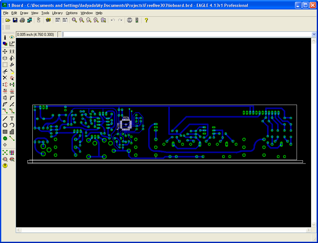
This is the PCB we'll be making a stencil for. It only has one chip but of course you can use a more complex layout
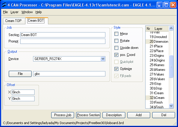
Your PCB software should be able to create/export the Cream Layer (solder paste layer) in Gerber RS274x format. In Eagle you can make your own Job for this quite easily
Also export the Dimension layer (PCB outline) since that will help a lot in registration
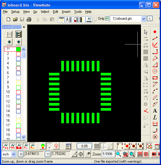
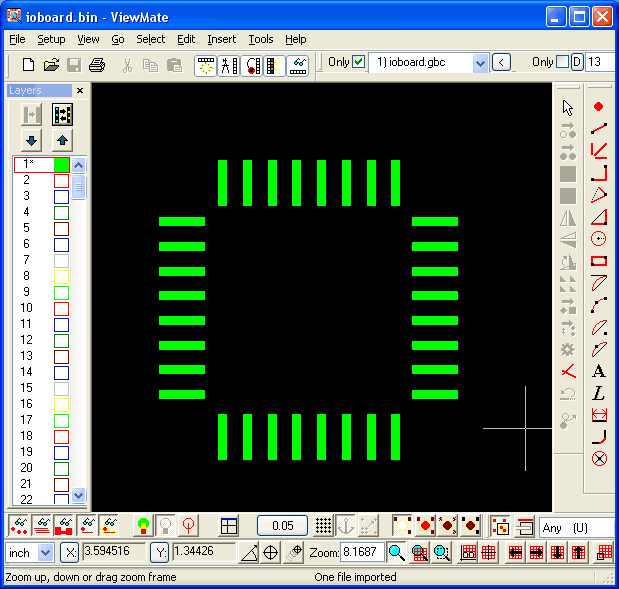
Import cream Gerber in Viewmate
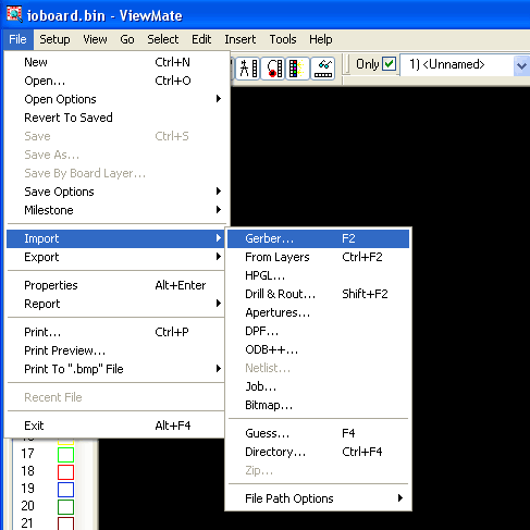
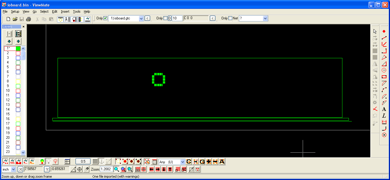
Start up Viewmate and File>Import>Gerber one of the Gerber files generated
You can zoom in using the Magnifying glass tool
Swell pads
Next we will make minor adjustnents to shrink the pads a little
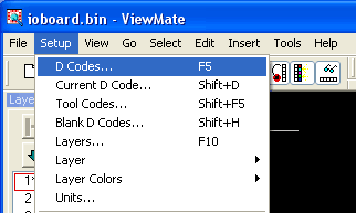
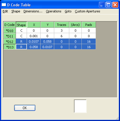
Select Setup>D Codes
Which will bring up a list of all the pads used. You will probably just want to select all of them
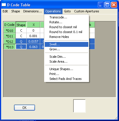
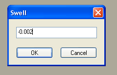
Then select Operations>Swell
and input somewhere around -0.002 (2 mil) to shrink all the pads by 0.002 inches in each direction
You'll now see that your pads are thinner. This prevents bridging since the laser is not perfectly precise and tends to 'go over' the boundaries by a few mils.
Export
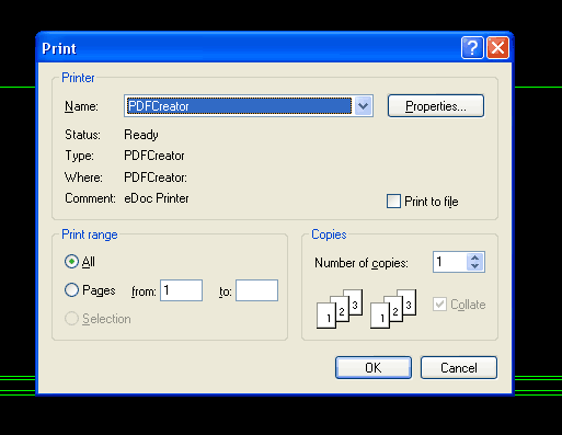
Now we'll export to PDF which will allow for easy importing into Corel Draw. The free version of Viewate doesnt seem to permit exporting, but you can print to PDF which is just as good.
Cut!
Import into Corel Draw and use raster not vector, to burn away the kapton film. For a 35W or 45W epilog, 30% speed and 100% power at 600 dpi made for a nice clean edge. Be sure to gently rub the stencil with water and a paper towel to get rid of the burnt kapton.
I usually use the Dimension layer info to make a jig for silkscreening by cutting out the PCB outline in a 0.062'' (1/16th) clear acrylic sheet
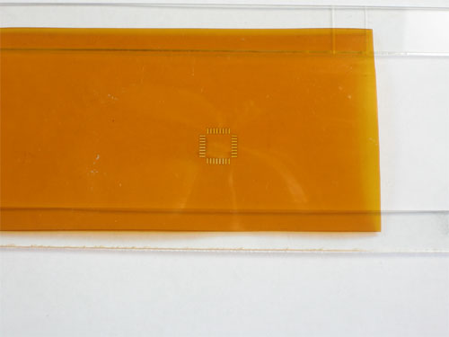
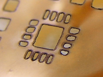
Here is a LFCSP 16 (4mm on each side) cut out of 2 mil kapton as above

